NanoDCAL Software

nanoacademic

nanodcal

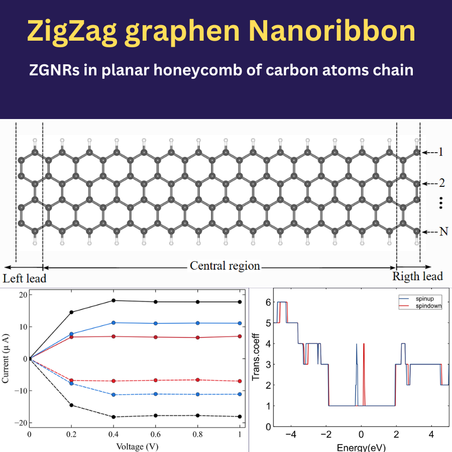
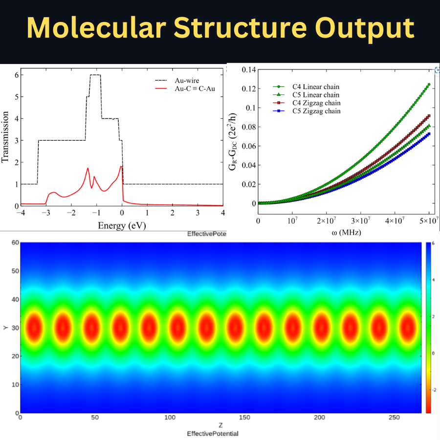
NanoDCAL is a state-of-the-art first principles quantum transport package, combining the nonequilibrium Green’s functions (NEGF) formalism with density functional theory (DFT) that predicts nonequilibrium quantum transport in nanostructures.

  • Written in MATLAB and C
  • Molecular and nanoscale electronics
  • Spintronics (collinear / non-collinear / spin-orbit coupling)
  • Semiconductor nanoelectronics (I-V curve)
  • Graphene & other 1D-2D Material.
  • Material Science & Chemistry.
  • Phonons calculations
  • Study molecules, crystals, one-probe two or multi-probe systems
  • Force, stress, structure optimization
  • Electron-phonon coupling
  • Photocurrent
  • Thermal transport coefficients.

nanodcal

Applications

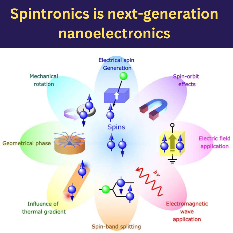
Physical and chemical properties of materials based on the spin-dependent states (collinear) in ferromagnetic (FM) or anti-ferromagnetic (AFM) configurations, the Kohn-Sham single-particle wave functions are represented as products of spatial orbitals with up- or down-spinors. The magnetic moment from the system is collinear with spin quantization axis. The first-principles density functional theory (DFT) with the local density approximation combined with the nonequilibrium Green’s function (NEGF) formalism as implemented in the NanoDCAL.


Electronic structure of DFT+U of NiO

Download PDF

View Youtube Video

Transmission spectrum of spin-polarized atomic chain

Download PDF

View Youtube Video

Electric transport of nickel black phosphorus nickel

Download PDF

View Youtube Video

Calculation of non-collinear spin of metal nanowires

Download PDF

View Youtube Video

Zigzag graphene nanoribbon

Download PDF

Semiconductors are an amazing class of materials with tunable electrical conductivity. The advances in semiconductor technology are devoted to exploring these materials to convert them into carefully-designed functional devices with the targeted electrical and optical properties. The miniaturization of those devices becomes one of the main trends in the future semiconductor industry. These tutorials and videos focus on how to set and compute the outstanding physical-chemical properties of several semiconductors.


Spin-orbit coupling splitting in semiconductor energy bands

Download PDF

View Youtube Video

Effective carrier mass in silicon materials

Download PDF

View Youtube Video

Calculation of complex energy band

Download PDF

Bi2Se3 topological insulator

Download PDF

View Youtube Video

Transport characteristics of semiconductor devices

Download PDF

View Youtube Video

HfO2SiO2 heterojunction VBO calculation

Download PDF

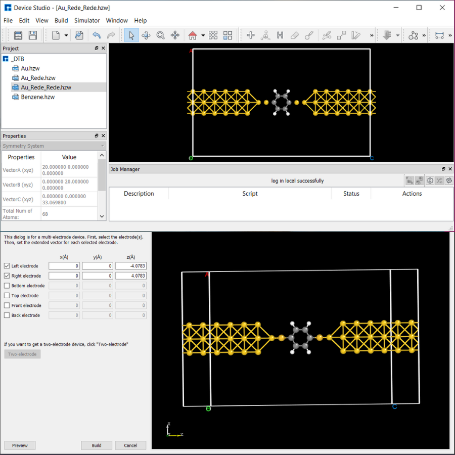
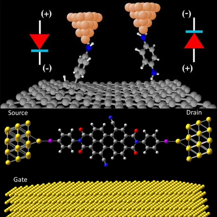
Molecular electronics is a field of study that deals with the design, fabrication, and application of electronic devices that are based on individual molecules or molecular assemblies. One of the main goals of molecular electronics is to develop devices that are smaller, faster, and more energy-efficient than conventional electronic devices. This is because molecules can be arranged in much smaller and more precise patterns than bulk materials.

Some of the potential applications of molecular electronics include:

  • New types of transistors: Molecular transistors could be used to create electronic devices that are much smaller and faster than conventional transistors.
  • New types of sensors: Molecular sensors could be used to detect a wide variety of chemicals and biological molecules.
  • New types of batteries:Molecular batteries could be used to store energy in a much more efficient way than conventional batteries.

Molecular device simulation tutorial

Download PDF

View Youtube Video

Al-C9H5NS2-Al molecular device transport

Download PDF

View Youtube Video

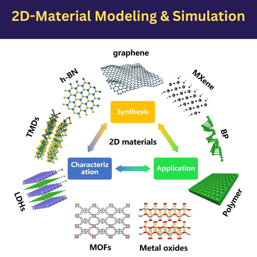
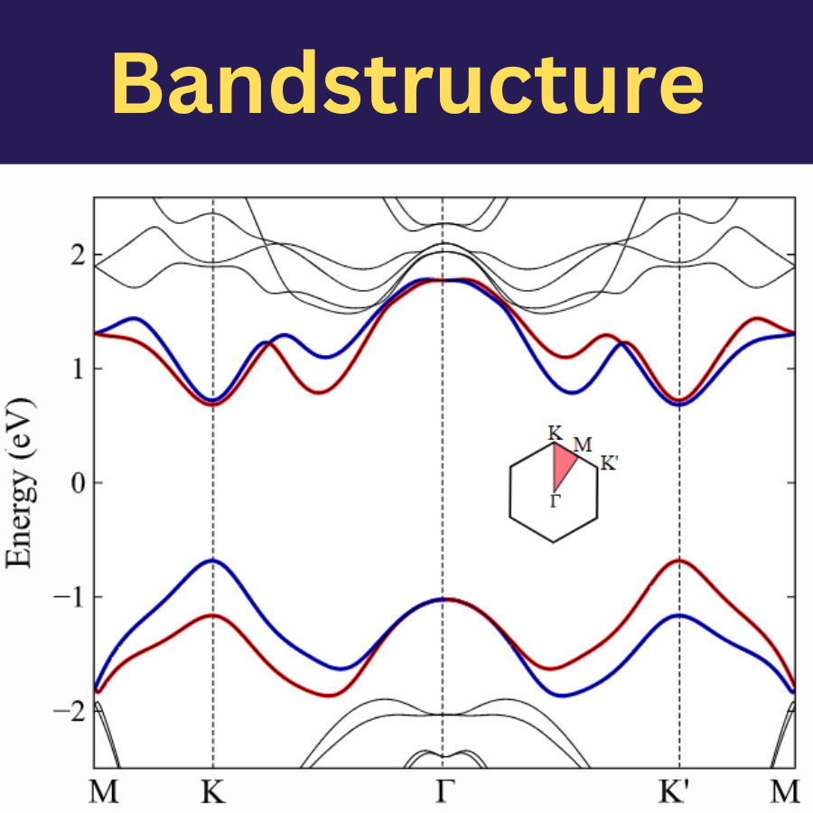
Two-dimensional (2D) materials can be defined as a crystalline structure that consists of a single- or few-layer of atoms. In fact, those materials can be described as a “hybrid” system of a solid (in the periodic plane) and a molecule (nonperiodic perpendicular direction). The atoms along the in-plane directions are strongly bonded by covalent or ionic interactions to form the atomic layer and the electrons are free to move throughout the plane. On the other hand, along the out-of-plane direction, these atomic layers are weakly held by van der Waals force, in that case, the movement of the electrons is restricted and governed by quantum mechanics.


Transmission spectrum of perfect graphene and MoS2 sheets

Download PDF

View Youtube Video

Opening the band gap of double-layer graphene under an electric field

Download PDF

View Youtube Video

Spin-resolved Bloch states in graphene

Download PDF

Transport in graphene nanoribbons

Download PDF

View Youtube Video

Graphene nanoribbon devices electrical properties

Download PDF

View Youtube Video

Material science and chemistry deal with the study of materials and their properties, structure, composition, and behavior. While material science focuses on understanding the structure-property relationships of various materials, chemistry delves into the composition, reactions, and behavior of substances at the molecular and atomic levels.


Visualization of LUMO_ HOMO orbits of water molecules

Download PDF

View Youtube Video

The relativistic effect of bulk gold

Download PDF

View Youtube Video

Generation energy

Download PDF

Si(100) surface reconstruction, geometric structure optimization

Download PDF

View Youtube Video

Silicon under uniaxial and biaxial stress

Download PDF

View Youtube Video

CoPd (100) structure optimization

Download PDF

Formation energy of charged point defects (manual method)

Download PDF

Controlling work function of silver surface by depositing ultra-thin oxide layer

Download PDF

Greens function method to simulate material surface

Download PDF

Using ghost atoms to calculate surface work function

Download PDF

We’re Delivering the best customer Experience